
Veteran testing giant Amkor is stepping up its layout! Chiplet, the battle of the chip giants.

Amkor is striving to firmly grasp the technological discourse and first-mover advantage in the field of Chiplet, which is considered the most core technology area in the "post-Moore's Law era".
According to the Zhongtong Finance APP, Amkor Technology, a veteran leader in the semiconductor testing industry established in 1968, recently announced that its newly built advanced chip packaging plant in Bac Ninh, Vietnam, with an investment of up to $1.6 billion, has officially opened on the 11th local time. Amkor stated that the Vietnam factory will become its largest factory in terms of area, covering 57 acres in the Yen Phong 2C Industrial Park. Once fully completed, it will have 200,000 square meters of cleanroom space. The factory will start with advanced system-level packaging (SiP) and memory production, providing one-stop turnkey solutions from design to electrical packaging testing for leading semiconductor and electronic manufacturing companies worldwide.
Regarding Amkor's decision to expand its presence in the advanced packaging field, industry insiders generally believe that due to the continued strong demand for NVIDIA A100/H100 GPU chips and the insufficient supply of Taiwan Semiconductor Manufacturing Company's (TSMC) CoWoS advanced packaging capacity in the coming quarters, NVIDIA and TSMC may transfer part of their advanced packaging capacity demand to Amkor's factories.
Currently, TSMC relies on its leading advanced packaging technology to secure a large number of high-performance chip packaging orders, but its advanced packaging capacity cannot keep up with the demand. The limited CoWoS advanced packaging capacity is the reason why NVIDIA H100 cannot meet the demand. Research institution TrendForce predicts that the CoWoS packaging capacity will remain tight in the second half of the year, and strong demand will continue until 2024. In addition, Amkor's new factory in Vietnam is expected to drive local economic development and make Vietnam a rising global semiconductor supply chain center.
Giel Rutten, President and CEO of Amkor, stated that the advanced packaging plant in Vietnam not only supports the global semiconductor supply chain but also supports regionalized semiconductor supply chains. "In the communication, automotive, high-performance computing, and other critical technology industries, customers need this secure and reliable supply chain."
Amkor's $1.6 billion investment in expanding its testing and packaging business in Vietnam means that the company is following in the footsteps of chip giants such as TSMC, Intel, and Samsung Electronics in the development of the Chiplet field, striving to firmly grasp the technological discourse power and first-mover advantage in this core technology field of the "post-Moore era."
Chiplet advanced packaging technology - the core part of SiP
Chiplet advanced packaging technology can be said to be the core and fundamental technology for achieving SiP. SiP refers to the packaging as a whole after all the processes are completed, and it can be said that there is no SiP without the foundation of Chiplet packaging technology.
It is understood that this veteran testing giant, established in 1968, has been paying attention to advanced system-level packaging (SiP) and investing in it since 2017. In June 2017, Amkor announced the establishment of a division called " The new department of "SiP Solutions" aims to accelerate the research and large-scale adoption of SiP products.
Currently, there are several mainstream paths for implementing advanced System-in-Package (SiP) technology: 2D SiP, 3D SiP, COWOS (Chip on Wafer on Substrate), Fan-Out SiP, InFO (Integrated Fan-Out), and EMIB (Embedded Multi-die Interconnect Bridge). These mainstream paths are all based on the advanced packaging technology of Chiplets.
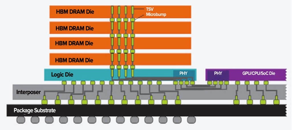
NVIDIA relies on TSMC's 2.5D CoWoS packaging technology, which is based on the Chiplet concept, and Amkor's advanced packaging factory in Vietnam is expected to take on some of the production capacity.
From the disassembly diagram of the H100 accelerator system, it can be seen that the H100 integrates SK Hynix's HBM high-performance memory and GPU core using TSMC's CoWoS packaging technology. The H100 GPU chip system combines TSMC's 4nm process and Chiplet packaging technology. NVIDIA integrates the HBM3 subsystem into the chip system using Chiplet technology, providing up to 3TB/s of ultra-high memory bandwidth, nearly twice the bandwidth of the previous generation product. At the same time, with TSMC's 4nm process, there is a significant improvement in performance, data transmission, and storage capacity compared to the previous generation A100 GPU chip.
As Moore's Law approaches its limits, Chiplet advanced packaging comes to the rescue.
In the "Post-Moore Era" we are in, breaking through the advanced chip manufacturing process faces great difficulties (such as quantum tunneling effects) and extremely expensive technology development costs. Giants like TSMC also find it difficult to bear high expenses.
As we enter the AI era and the trend of everything being interconnected becomes more apparent, the demand for computing power from various tasks may skyrocket. For example, deep learning tasks, as well as machine learning, inference, AI-driven image rendering, and recognition, all have very high hardware performance requirements. This means that standalone CPU or GPU integration, like in PCs, can no longer meet the computing power demands.
Therefore, Chiplet advanced packaging technology has emerged. This technology allows for the integration of different "chip processing units," or different "Chiplet cores," to meet diverse computing needs and optimize performance. In addition, due to the diversity of AI applications, hardware optimization is often required for specific tasks. Different processing unit chips can be specifically used for specific types of calculations, such as image processing, speech recognition, natural language processing, etc. The modular design based on the Chiplet concept allows for the selection of the best processing unit for each task.
Chiplet, the battle of chip giants
Chiplet advanced packaging seems to have become a new battlefield for chip giants. Intel, Samsung Electronics, and TSMC have all invested heavily in this technology sector. From the perspective of the chip industry chain, as Chiplet packaging technology becomes more popular, it will bring about an innovation to the entire industry chain, especially for chip manufacturing equipment suppliers and packaging and testing companies. They will explore new business directions and provide innovative manufacturing support for Chiplet packaging. For example, Applied Materials, a global chip equipment giant and an upstream equipment supplier for chip manufacturers such as TSMC, recently announced two new technologies related to wafer Hybrid Bonding and Through Silicon Via (TSV), which will help improve the 2.5D and 3D Chiplet packaging processes. The new solutions expand the range of Applied Materials' heterogeneous integration (HI) technology.
Based on Chiplet advanced packaging technology, more GPUs or other types of chips can be integrated to meet the increasing demand for computing power. Many AI tasks involve large-scale parallel computing, such as neural network system training and inference. GPUs and other processors perform well in parallel computing, and Chiplet packaging technology can enable different GPU modules, or CPU, FPGA, ASIC chips, etc., to work together in the same chip system to provide larger-scale parallel computing capabilities.
Currently, Intel is building its latest packaging plant in Penang, Malaysia, to strengthen its 2.5D/3D packaging layout. This will be Intel's first 3D packaging plant outside the United States to adopt Intel's Foveros advanced packaging architecture, following its factories in New Mexico and Oregon. Intel stated that its planned capacity for 3D Foveros packaging will be four times the current level by 2025. Through years of research and exploration, Intel is currently focusing on various advanced packaging technologies based on the Chiplet concept, such as 2.5D EMIB and 3D Foveros, aiming to achieve the goal of doubling interconnection bandwidth and halving power consumption through forms of HI technology such as 2.5D, 3D, and embedded. According to reports, Samsung Electronics' fourth-generation HBM and packaging services have been tested by AMD. AMD's Instinct MI300 series AI chip system is planned to adopt Samsung's HBM3 and Chiplet packaging services, which will integrate the central processing unit (CPU), graphics processing unit (GPU), and HBM3. It is expected to be released in the fourth quarter of this year. In order to compete for future chiplet packaging market share, Samsung is developing more advanced I-cube and X-cube packaging technologies.
According to the latest research report from well-known research institution Markets And Markets, the total market size of advanced packaging technologies for chiplets covering GPUs, CPUs, FPGAs, and others, as well as advanced packaging technologies (2.5D/3D, COWOS, and Fan-Out), and the chiplet market is expected to reach approximately $148 billion by 2028, with an astonishing compound annual growth rate (CAGR) of 86.7%. According to the institution's calculations and estimates, the overall market size of chiplets in 2023 may be only $6.5 billion.
