
Taiwan Semiconductor 2nm, quietly in mass production

Taiwan Semiconductor has begun mass production of its N2 (2nm) process chips, although no official press release has been issued. The N2 process utilizes first-generation nanosheet transistor technology, expected to achieve a 10%-15% performance improvement and a 25%-30% reduction in power consumption. This technology will become the most advanced in the semiconductor industry, further consolidating Taiwan Semiconductor's technological leadership
Taiwan Semiconductor Manufacturing Company (TSMC) quietly announced that it has begun mass production of chips using its N2 (2nm) process. The company did not issue a formal press release to announce the start of mass production, but it had previously stated multiple times that the N2 process was expected to achieve mass production in the fourth quarter, thus this plan has been realized.
TSMC stated on its 2nm technology webpage: "TSMC's 2nm (N2) technology is on track to begin mass production in the fourth quarter of 2025."
The N2 process employs first-generation nanosheet transistor technology, achieving full-node improvements in performance and power consumption. TSMC has also developed low-resistance redistribution layers (RDL) and ultra-high-performance metal-insulator-metal (MiM) capacitors to further enhance performance.
TSMC's N2 technology will become the most advanced technology in the semiconductor industry in terms of density and energy efficiency. With its leading nanosheet transistor structure, the N2 technology will deliver full-node performance and power consumption advantages to meet the growing demand for energy-efficient computing. Through our ongoing improvement strategy, N2 and its derivative technologies will further solidify TSMC's technological leadership and keep it ahead for a long time to come."

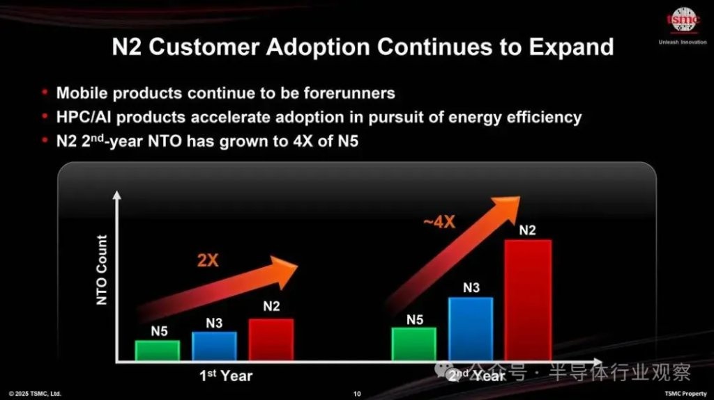
From the perspective of performance improvement, the design goal of N2 is to achieve a 10%-15% performance increase at the same power consumption, a 25%-30% reduction in power consumption at the same performance, and a 15% increase in transistor density compared to N3E for mixed designs that include logic, analog, and SRAM. For pure logic designs, the transistor density is 20% higher than N3E.

TSMC's N2 process is the company's first process node to use gate-all-around (GAA) nanosheet transistors. In this type of transistor, the gate completely surrounds the channel made up of horizontally stacked nanosheets. This geometric structure improves electrostatic control, reduces leakage current, and enables smaller transistor sizes without sacrificing performance or energy efficiency, ultimately increasing transistor density. Additionally, the N2 process incorporates ultra-high-performance metal-insulator-metal (SHPMIM) capacitors into the power delivery network. These capacitors have a capacitance density more than twice that of the previous generation SHDMIM design and reduce thin-film resistance (Rs) and via resistance (Rc) by 50%, thereby improving power stability, performance, and overall energy efficiency.
TSMC CEO C.C. Wei stated during the company's earnings call in October: "The mass production of N2 chips is progressing smoothly and is expected to be realized later this quarter, with good yields. We anticipate that the ramp-up in capacity will accelerate in 2026, driven by smartphone and high-performance computing AI applications." Interestingly, Taiwan Semiconductor Manufacturing Company (TSMC) has begun producing 2-nanometer chips at its Fab 22 facility near Kaohsiung, Taiwan. Previously, the market expected TSMC to start ramping up production capacity for N2 process chips at its Fab 20 facility (located near Hsinchu, Taiwan), which is adjacent to its new global R&D center where the N2 series process technology was developed. Mass production at Fab 20 may be slightly delayed.
TSMC will conduct large-scale mass production of N2 process chips at the brand-new wafer fab, which always presents certain challenges. Notably, the company will simultaneously mass produce smartphone chips as well as larger "artificial intelligence" and "high-performance computing" chips at the new wafer fab (it is important to note that high-performance computing is a broad concept that encompasses various applications, from gaming console SoCs to high-performance server CPUs), which will add some additional complexity. Typically, TSMC prioritizes mass production of mobile and small consumer-grade chips.
The simultaneous construction of two wafer fabs with N2 process capabilities is due to the strong interest from TSMC's numerous partners in this new process technology, necessitating sufficient capacity for all partners. Additionally, starting from the end of 2026, these two wafer fabs will be used to produce chips based on N2P (an enhanced version of the N2 process) and A16 (an upgraded version of the N2P process, featuring Super Power Rail back power supply design, specifically designed for complex AI and HPC processors).
Wei added, "In line with our strategy of continuous improvement, we will launch N2P as an extension of the N2 series products. N2P further enhances performance and power consumption based on N2, with mass production planned for the second half of 2026. Additionally, we have introduced A16, which utilizes our top-tier Super Power Rail (SPR). A16 is best suited for specific high-performance computing (HPC) products with complex signal paths and dense power delivery networks. Mass production of A16 is also proceeding as planned, set to commence in the second half of 2026."
Risk Warning and Disclaimer
The market has risks, and investment should be cautious. This article does not constitute personal investment advice and does not take into account the specific investment objectives, financial situation, or needs of individual users. Users should consider whether any opinions, views, or conclusions in this article align with their specific circumstances. Investment based on this is at one's own risk
